Keep an eye out for Resistive Random-Access Memory (ReRAM), an up-and-coming type of computer memory technology. ReRAM is currently under development by a number of companies—including Panasonic, HP, Adesto Technologies, and Crossbar, among others. It is the likely replacement for, and massive improvement upon, Flash memory. At the moment, the costs and performance of ReRAM are not at a level that makes the technology ready for the mass market. But, there is a tremendous potential in this type of memory device, and it is on the verge of becoming a part of the digital mainstream.
What is it?
To put it very simply, ReRAM memory device is based on a three-layer structure: two outer layers of electrode material and an inner layer of some type of dielectric material, referred to as a memristor. When an electric current is applied, the resistance of the dielectric material changes. This change of resistance can be measured and read as a 1 or a 0. ReRAM is a memory type known as non-volatile. This means that the device can hold saved data even when the power to the device is turned off.

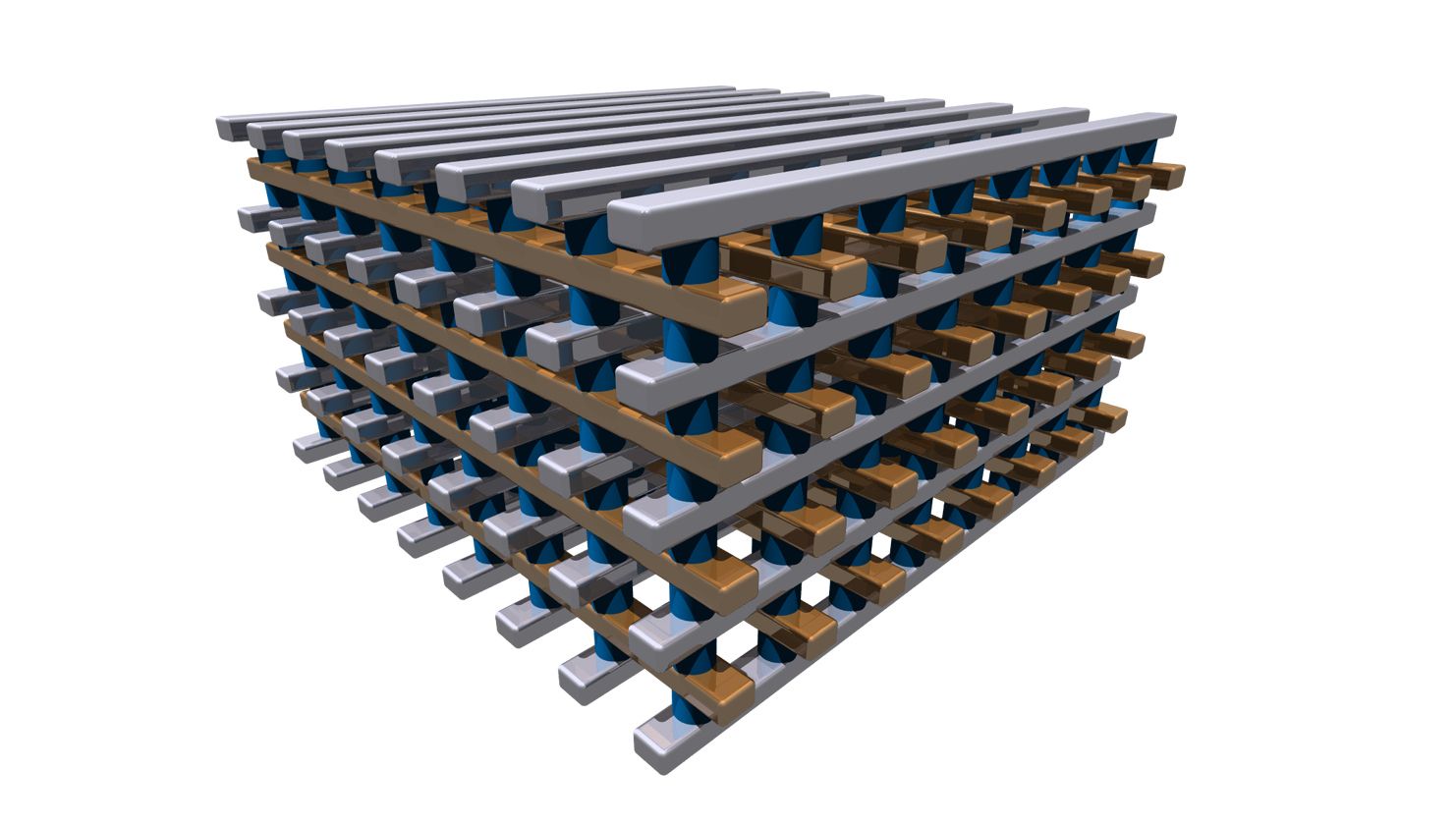
ReRAM three-layer structure. Image courtesy of Crossbar.
Why do we need it?
Flash memory, found in the familiar USB memory sticks we all use, is also a non-volatile type, but ReRAM offers some significant advantages over Flash.
Compared to Flash, ReRAM is much faster. According to Crossbar, one of the major players in the race to bring the technology to the masses, the new memory tech delivers 100 times lower read latency and 1000 times faster write performance than Flash. It has 20 times lower power consumption than NAND Flash, and lasts 1000 times longer–that adds up to many more read-write cycles. ReRAM is made with CMOS-friendly materials and can be made with standard manufacturing processes.
And then there is perhaps the biggest advantage: The potential for massive amounts of storage in unbelievably small amounts of space. We’ll let Crossbar explain this.
Crossbar ReRAM technology can be stacked in 3D, delivering multiple terabytes of storage on a single chip. Its simplicity, stackability and CMOS compatibility enable logic and memory to be integrated onto a single chip at the latest technology node (see lead image at the top of this article).
Crossbar’s patented built-in selector allows various memory array configurations in which a single transistor can drive one or thousands of memory cells. This enables Crossbar cells to be organized in super dense 3D cross-point arrays, stackable with the capability to scale below 10nm, paving the way for terabytes on a single die.
It could very well be the future of memory. And it could become a big part of your life soon. Learn more here.


